
As semiconductor manufacturing advances, 3D chip stacking and advanced packaging are becoming essential for increasing performance, power efficiency and miniaturization. However, these innovations present significant metrology challenges, as traditional measurement techniques struggle to inspect multi-layer structures with the necessary precision. Erik Hosler, an expert in semiconductor process control and metrology, emphasizes that cutting-edge metrology solutions are required to ensure accuracy, reliability and yield in 3D integration.
Challenges in Metrology for 3D Chip Stacking
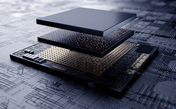
Unlike traditional planar semiconductor fabrication, 3D integration involves stacking multiple layers of logic, memory and interconnects, requiring through-silicon vias (TSVs), hybrid bonding and advanced interposers. Each of these elements introduces new complexities in metrology, including:
Alignment Accuracy: Precise bonding is essential for 3D-stacked devices. Even the slightest misalignment between layers can lead to performance failures.
TSV Inspection: Ensuring that TSVs are properly etched, filled and free of voids or cracks is critical for maintaining electrical integrity.
Hidden Defect Detection: Traditional surface-level metrology is insufficient for inspecting buried interfaces within stacked chips.
Thermal and Mechanical Stress Analysis: Stacked architectures introduce stress and warpage, requiring metrology tools that can assess structural integrity at the atomic level.
Emerging Metrology Solutions for 3D Integration
To address these challenges, fabs are implementing next-generation metrology tools capable of non-destructive, high-resolution inspection of complex 3D architectures. Some of the most promising advancements include:
X-ray Computed Tomography (XCT): This technique allows for non-invasive, high-resolution imaging of internal structures, making it ideal for inspecting TSVs and interconnects.
Optical Coherence Tomography (OCT): Used for layer alignment verification, OCT provides precise depth measurements without requiring physical cross-sections.
Acoustic Metrology: By utilizing ultrasonic waves, this method detects voids, delamination and stress fractures deep within stacked chips.
AI-Driven Metrology Optimization: Machine learning models are being integrated into metrology workflows to enhance pattern recognition, predict failures and optimize inspection parameters in real-time.
AI and Automation: Improving Yield and Efficiency
As metrology tools evolve, the integration of artificial intelligence and automation is enhancing both accuracy and scalability. AI-driven algorithms analyze large datasets from wafer inspections, improving defect classification and process control.
Erik Hosler observes, “AI takes the human out of the optimization iteration cycle, allowing the user to specify the performance criterion they are seeking and allowing AI to minimize the design to meet those requirements.” This capability ensures that 3D packaging techniques can be refined with greater precision and consistency, reducing yield loss and improving production efficiency.
The Future of Metrology in Advanced Packaging
With heterogeneous integration and chiplet architectures driving the next wave of semiconductor advancements, metrology must continue to evolve. The industry is investing in quantum-scale imaging, hyperspectral analysis and advanced in-line monitoring techniques to keep pace with the increasing complexity of 3D semiconductor packaging.
By leveraging these innovations, manufacturers can ensure high yield, enhanced reliability and long-term performance for next-generation semiconductor devices. As 3D integration becomes the standard, metrology will remain a critical enabler, ensuring that semiconductor advancements continue to push the boundaries of performance and efficiency.